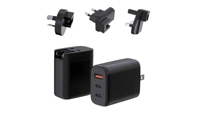
Two chargers with the same wattage can differ 30% in unit cost and weeks in lead time — the difference lives in the bill of materials. For OEM buyers, a BOM review is one of the fastest ways to judge a supplier's quality system, because every test result and delivery date traces back to the parts on that list.
The component map of a modern GaN charger
A modern GaN charger's BOM is led by five cost- and quality-critical groups: the GaN power IC, the PD/PPS controller, the transformer and magnetics, the capacitors, and the enclosure with its mechanical parts. The rest — resistors, connectors, PCB and protection devices — matters for reliability, but these five decide the product's performance envelope.
- Power stage: GaN ICs and synchronous-rectifier MOSFETs that convert and regulate power.
- Control: the USB PD/PPS protocol controller that negotiates voltage and current with the device.
- Magnetics: transformer, common-mode chokes and inductors — the largest and most custom parts.
- Capacitors: input bulk caps, output caps and EMI filter caps.
- Mechanical & thermal: PCB, housing, thermal pads or potting, connectors and cable.
The cost split is not equal: the GaN IC, transformer and enclosure typically account for the largest share of a 65W-class BOM, while capacitors and discrete parts add less cost but disproportionate reliability risk. As wattage climbs toward 140W and 240W, the transformer and power-stage devices grow in cost and lead time, and thermal materials (potting, shields, pads) start to appear as significant line items. This is why a 20W BOM and a 240W BOM are different products in everything except the label.
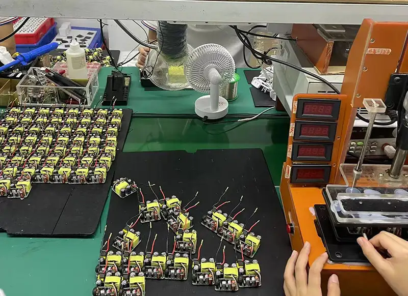
GaN ICs: vendors, specs and allocation risk
The GaN device is the heart of the BOM, and GaN ICs with integrated drivers have largely replaced discrete GaN FETs in compact chargers. Key specs are the voltage class (typically 650V), on-resistance, switching frequency, and whether driver, control or protection is integrated.
The sourcing risk is real: GaN devices are made by a limited set of vendors, and allocation and lead-time swings hit the power stage first when demand surges. A competent supplier keeps a primary and secondary qualified GaN source, and can name both in a BOM review. If a factory can only name one vendor and cannot qualify an alternative, your program inherits that risk.
When comparing GaN devices, look past the brand name at four numbers: voltage class (650V is the charger standard), on-resistance (lower means less conduction loss), switching frequency capability, and whether the driver is integrated. Integrated driver-plus-switch ICs shrink the board and simplify layout, but they also concentrate more risk in one part — so the device's qualification history and the supplier's second-source plan deserve the same scrutiny as the price. A design that qualifies a second GaN source at sample stage can switch vendors without redesigning the board; one that cannot is exposed to the next allocation cycle.
Magnetics, capacitors and the parts that fail first
After the GaN IC, the transformer is the most performance-critical and custom component: core material, winding layout and shielding are tuned per design, which is why custom transformers drive long lead times. Capacitors are the parts that age fastest — electrolytic capacitors degrade with heat and ripple current, so their brand, temperature rating and derating policy are quality signals. Ceramic capacitors on the output side handle ripple but are sensitive to DC bias and cracking.
In practice, field failures in chargers most often trace to capacitors, solder joints and connectors — not to the GaN die itself. That is why component choice and assembly quality matter as much as the headline semiconductor.
Transformer construction is where engineering choices become visible: core geometry (PQ or EE), winding arrangement, copper versus litz wire, and shielding layers all change efficiency, EMI and thermal behavior. A planar transformer can be thinner but costs more to tool; a conventional wound transformer is cheaper but larger. Similarly, ceramic capacitors on the output suffer DC-bias capacitance loss that can reach tens of percent at rated voltage — a spec that looks fine at zero bias can underperform in the real product. These details are exactly what a BOM review should surface.
Why BOM quality shows up in test results
Component quality is visible in factory test results long before it shows up in the field. A BOM using grade-screened capacitors and properly rated transformers will hold efficiency, stay inside EMI limits and pass load aging; a cost-cut BOM fails or passes marginally on exactly those tests.
That is why our quality-control gates run 100% electrical and functional testing plus load aging on every production batch, with per-batch inspection reports. When a supplier can show consistent test data, it is usually because the BOM is stable and qualified — not because the tests are lenient.
A concrete example: two 65W designs with the same GaN IC but different bulk capacitor brands can show nearly identical performance on paper and diverge after load aging — one holds efficiency and ripple, the other drifts as capacitance and ESR degrade under heat. EMI margins behave the same way: a transformer wound with different shielding can move conducted-emission results by several dB, flipping a design from pass-with-margin to marginal. Test reports reveal these differences; spec sheets hide them.
How component choices move cost and lead time
BOM cost is concentrated in the GaN IC, transformer and capacitors, while lead time is driven by the custom transformer and the availability of power-stage parts. A standard GaN IC with a stock transformer can be assembled quickly; a custom transformer and a scarce GaN device can add weeks.
| BOM area | Cost impact | Lead-time impact | Quality signal |
|---|---|---|---|
| GaN IC | High | Medium–high | Vendor brand, dual sourcing |
| Transformer (custom) | Medium | High | Core material, design validation |
| Electrolytic capacitors | Low–medium | Medium | Temperature rating, brand |
| PCB & assembly | Medium | Medium | Solder quality, ESD control |
| Enclosure & tooling | Medium | High (first order) | Tooling ownership, finish quality |
Using a BOM review as a supplier qualification step
Before committing volume, run a BOM review under NDA: request the full component list with vendor names, part numbers and datasheets, then check for obsolete parts, single-sourced items and unexplained substitutes. A factory that resists sharing a BOM under NDA is a red flag; one that walks you through it with engineering rationale is demonstrating the OEM/ODM engineering depth you need for a reliable product.
Which components are hardest to source
GaN power ICs, custom transformers and high-voltage MLCCs are the usual pinch points. GaN allocation follows consumer and data-center demand; custom transformers have no stock alternative by definition; and MLCC supply has been cyclical for years. For a program with predictable volumes, ask which of these parts are single-sourced and what the supplier's buffer stock policy is.
Cost trade-offs between quality tiers
Every quality tier has a defensible place: an economy BOM with mainstream parts suits high-volume, price-driven SKUs, while a flagship BOM with grade-A capacitors, better thermal materials and a certified transformer suits premium products. The risk is paying economy prices and receiving a BOM that was quietly downgraded after samples.
Beyond the tier, ask about lifecycle management: which parts are near end-of-life, how long the supplier commits to a qualified BOM, and what happens when a component goes obsolete. Obsolete electrolytic capacitors or a discontinued controller force a re-qualification that can cost weeks of lead time and new certification runs. A supplier that actively manages component obsolescence protects your product's shelf life — a quality signal that shows up in the BOM review, not in the brochure.
Questions to ask about your charger's BOM
End any BOM discussion with these questions so the answers are documented in your RFQ record.
- Which GaN device does the design use, and is a second source qualified?
- Who makes the transformer, and is it validated for the full operating range?
- What are the capacitor brands, temperature ratings and derating rules?
- Which parts are single-sourced, and what is the buffer stock policy?
- What changes were made to the BOM between sample approval and production?
FAQ
What are the main components of a GaN charger?
The critical groups are the GaN power IC, the PD/PPS controller, the transformer and magnetics, input and output capacitors, and the enclosure with thermal materials. These five decide efficiency, size, cost and reliability.
Which GaN charger component fails first?
Electrolytic capacitors and solder joints are the usual weak points, because heat and ripple age them fastest. The GaN device itself is rarely the first failure in a well-designed charger.
Why does GaN IC sourcing matter for lead time?
GaN power devices come from a limited set of vendors and can swing into allocation when demand spikes. A supplier with a qualified second source protects your delivery schedule; a single-sourced design does not.
Can I get a supplier's BOM?
Yes — under NDA, serious factories share the full component list with vendor names and part numbers. If a supplier refuses or offers only a partial list, treat it as a qualification risk.
Evaluating a supplier's BOM or starting a charger program? Our engineering team reviews component choices openly under NDA and can show how factory testing validates each batch. Contact us with your wattage and volume targets to start the conversation.
This article is part of GaN Charger Manufacturing & Sourcing, the guide that covers this topic in decision order.