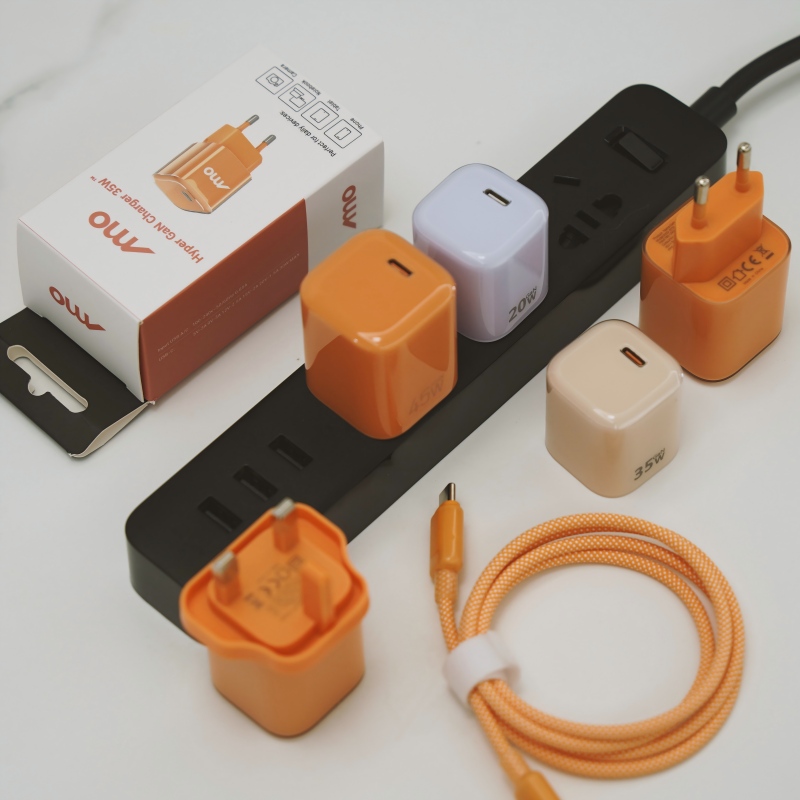
GaN chargers get smaller by switching faster, and faster switching is exactly what generates electromagnetic interference. For OEMs, EMI is not an afterthought: it decides certification timelines, component cost and whether a compact design passes CE and FCC the first time.
Why fast-switching GaN increases EMI risk
Every time a power switch turns on and off, it creates voltage and current transients that radiate energy — the same fast switching that fourth-generation GaN power ICs push to higher frequencies. GaN switches at megahertz frequencies with very fast edges — GaN devices operate above 1 MHz — which moves interference into frequency bands that are harder to filter and more likely to exceed emission limits.
The same properties that make GaN attractive — high frequency, high slew rate, compact layout — are the properties that create EMI. A compact board also packs the noise source closer to cables and connectors, which act as antennas. The result: EMI design is a first-order engineering task in every GaN charger, not a certification-stage fix.
The physics is worth understanding because it drives the fixes. Fast voltage edges (high dv/dt) couple energy into adjacent traces and the transformer, producing common-mode noise; fast current edges (high di/dt) create differential-mode noise across the input loop. Higher switching frequency shifts the spectrum upward, where filters are less effective and radiated coupling grows. That is why GaN designs cannot simply reuse a silicon charger's filter — the noise signature is different, and the filter, transformer and layout must be re-tuned for it.
Conducted vs radiated emissions
EMI splits into two paths that are tested differently.
- Conducted emissions: noise that travels back through the power cord into the mains, measured from 150 kHz to 30 MHz.
- Radiated emissions: energy radiated through the air from the board, cables and enclosure, measured from 30 MHz to 1 GHz and beyond.
Conducted noise is addressed with input filters and common-mode chokes; radiated noise depends on shielding, layout and cable management. Understanding which path fails a test tells you which design lever to pull.
The measurement setup matters too. Conducted testing uses a line impedance stabilization network (LISN) to make the mains impedance predictable; radiated testing uses antennas in an anechoic chamber or on an open-area test site. Both report against quasi-peak and average limits, and a design can pass average while failing quasi-peak or vice versa. When a supplier shares EMI plots, check which detector and which limit line they were measured against — the difference between "passed" and "passed with margin" is usually visible on the chart.
Shielding, filters and layout practices
Four design practices control EMI in a compact charger, in rough order of impact.
- Layout: keep the switching loop small, separate primary and secondary, and place the controller away from noisy traces.
- Input filtering: common-mode chokes and X/Y capacitors sized for the noise spectrum.
- Shielding: metal shields over the transformer and power stage, often combined with thermal roles.
- Snubbers and gate control: slow the switching edges just enough to cut high-frequency energy without losing efficiency.
Texas Instruments' power supply design seminar library covers EMI design for flyback and resonant converters in depth — including transformer construction and filter design, the two areas where most margin is won or lost.
In a compact GaN brick, the common-mode choke and Y capacitors are the workhorses of conducted filtering, and their value and placement are tuned to the noise spectrum. Change the transformer winding order or add a shield layer, and the common-mode signature changes enough to require re-tuning the filter. This coupling is why "copy the reference design" rarely works for EMI: the interaction between transformer, filter and layout is unique to each board.
How EMI shows up in CE/FCC testing
Compliance testing measures emissions against CISPR and FCC Part 15 limits. A design with good EMI margin passes with margin to spare; a marginal design fails, and the fix usually costs time and money in certification revisions.
| Emission path | Frequency range | Typical fixes |
|---|---|---|
| Conducted | 150 kHz – 30 MHz | Chokes, X/Y caps, transformer shielding |
| Radiated | 30 MHz – 1 GHz+ | Enclosure shielding, cable routing, layout |
Design choices that keep certification schedules
Certification re-runs are expensive, so the goal is to build margin in from the start. Pre-certification screening with a spectrum analyzer, an EMI-optimized transformer design and a fixed cable plan all reduce surprises at the test house.
- Choose components with known EMI behavior, not just cost.
- Validate layout with pre-compliance scans before sending samples to certification.
- Freeze the final cable and enclosure design before the formal test.
EMI questions for your manufacturing partner
Use these questions to judge whether a partner can actually deliver an EMC-clean product.
- What EMI margin did the last certification test show on this design?
- Can you share conducted and radiated emission plots from pre-compliance testing?
- Which filter components are on the BOM, and are they single-sourced?
- How does the layout change between a 65W and a 140W version?
- What happens to EMI when the enclosure or cable changes?
EMI standards: CISPR and FCC limits
The relevant limits come from CISPR standards (adopted in the EU as EMC requirements) and FCC Part 15 in the US, with regional variations in other markets — the IEEE overview of switched-mode power supply design explains how converters generate this noise. Certification coverage is model-dependent, so confirm which standards apply to each target market and each SKU.
Common EMI failures and fixes
The same failures appear again and again in charger development: excessive common-mode noise from transformer coupling, poor grounding between board and enclosure, and cables picking up board noise. Each has a known fix — transformer shielding tape, grounding springs and cable ferrites — which is why experience shows up as faster fixes.
Three scenarios illustrate the pattern. A conducted failure at low frequency usually traces to the input filter or transformer coupling, and a shield layer on the transformer plus a larger choke fixes it. A radiated failure at higher frequency often comes from a grounding gap between the board and a metal shield — add a grounding spring and the spike disappears. And the classic "passes on the bench, fails with the cable attached" case is the cable acting as an antenna; routing it differently or adding a ferrite returns the margin. Recognizing the signature is the skill that turns a two-week debugging cycle into a two-day fix.
How layout and shielding affect certification
Layout is the difference between a design that passes with 10dB margin and one that barely scrapes through. Shielding adds cost, so a good layout minimizes how much shielding you need. Ask for board photos and, where possible, a pre-compliance report before committing to a manufacturing partner with EMC experience.
EMI testing cost and timeline
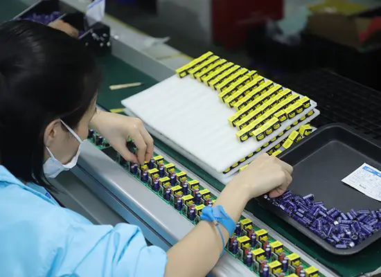
Formal EMI testing typically adds weeks to a project, and each failed run adds more. Pre-compliance screening is far cheaper than formal re-testing, so budget for it. Our factory and quality-control processes track test results per batch, giving buyers evidence that EMI behavior stays consistent in production — not just on the sample.
A typical timeline: pre-compliance scans and tuning during development, one formal test pass with margin, then production verification. The cost that surprises most teams is the failure loop — each failed formal run means re-tuning, re-spinning the board or adding components, and re-testing. Teams that build EMI margin in during layout, rather than chasing it at the test house, finish the loop once instead of three times.
Selecting a partner with EMC experience
Ask how many similar products a factory has certified, what margins they achieved and whether they own pre-compliance equipment. EMI is a design skill that accumulates over projects; a partner that treats it as a first-order constraint will protect your launch schedule.
FAQ
Do GaN chargers cause EMI?
All switching chargers generate EMI, and GaN's fast switching edges make the challenge bigger. Good layout, filtering and shielding keep emissions within CE and FCC limits.
How do you reduce EMI in a GaN charger?
Control the switching loop layout, add common-mode chokes and X/Y capacitors, shield the transformer, and manage switching edge rates. Pre-compliance testing verifies the fix before formal certification.
What is the difference between conducted and radiated emissions?
Conducted emissions travel back through the power cord and are measured from 150 kHz to 30 MHz; radiated emissions travel through the air and are measured from 30 MHz upward. They need different filters and shielding strategies.
Does a smaller charger have worse EMI?
Not necessarily, but compact layouts put the noise source closer to cables and connectors that act as antennas, so EMI control requires more deliberate design rather than being automatically worse.
Evaluating a charger design for certification readiness? Ask our engineering team for EMI margins and test evidence through the contact page — we build compact GaN chargers with EMC as a design input, not a certification surprise.
This article is part of GaN Chargers, the guide that covers this topic in decision order.